HELLO WORLD!!!
— NES 001 (@001NES) April 23, 2015
Background
In the late 80s I was in love with the NES, it blew my Intellivision and Atari 800XL away; at the time it seemed like a machine that was capable of infinite power. During that period there was one fateful night I examined the NES unit and noticed a small compartment at the bottom, upon removing the plastic guard I discovered it was an expansion port! My mind reeled with possibilities, what would Nintendo do with this amazing new interface we discovered?
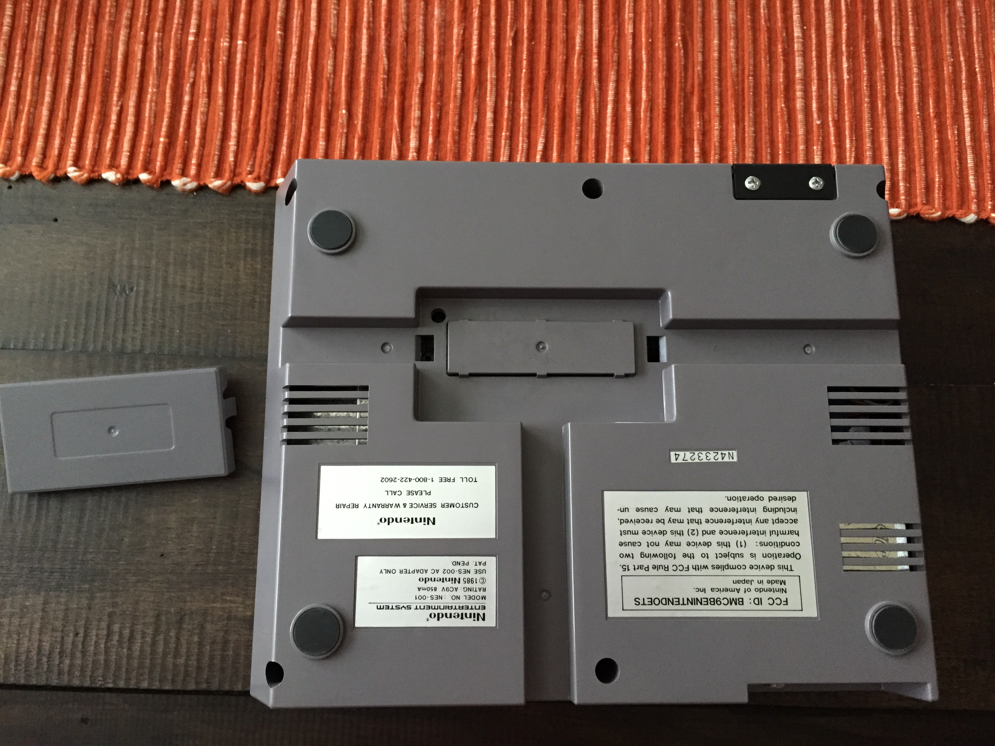
The expansion port with the plastic stab still attached
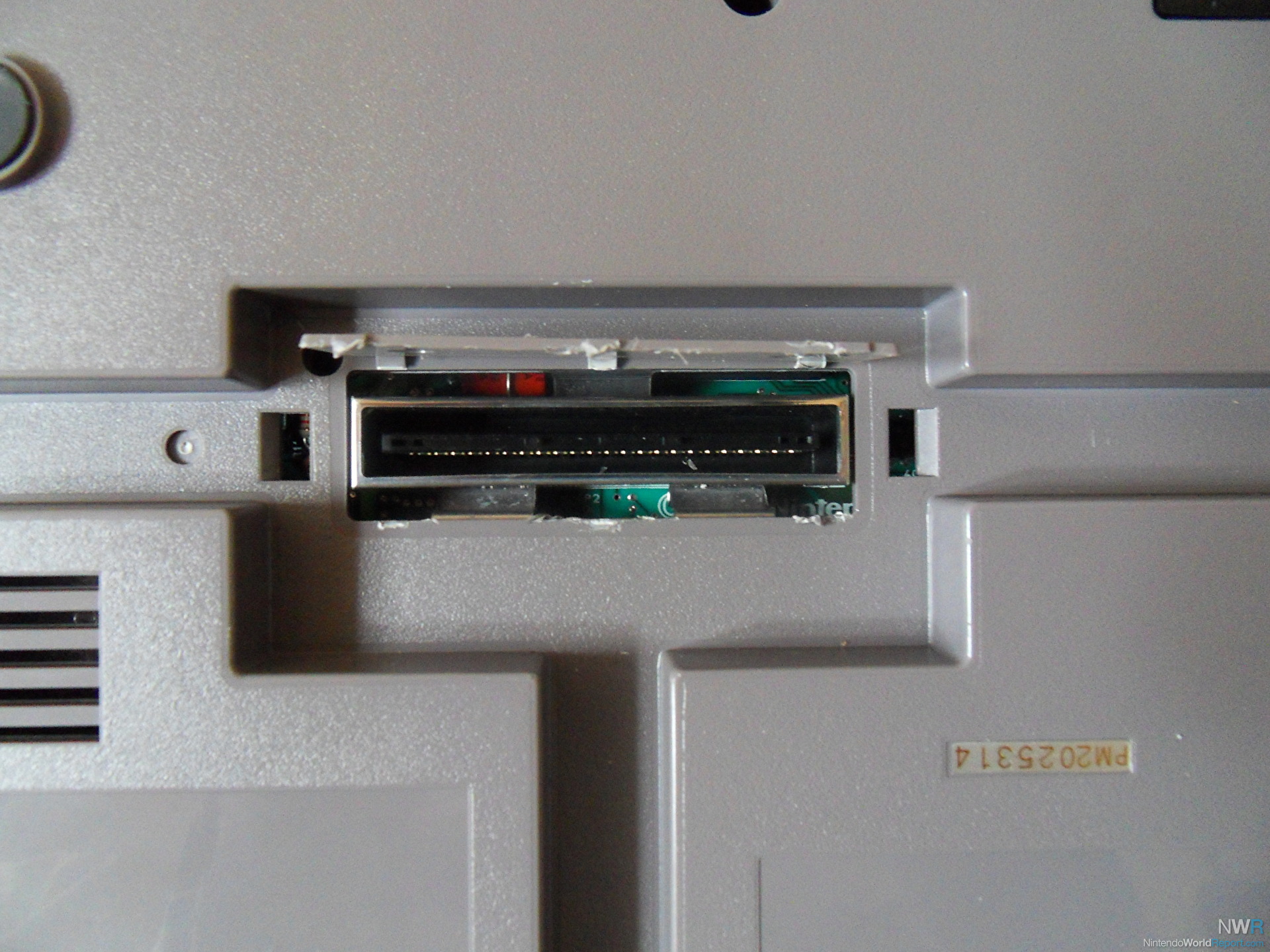
The expansion port with the tab removed, courtesy of www.nintendoworldreport.com
Fast forward to 2015. Nothing was ever officially done with the expansion port and it was removed in the later top loading revision of the NES. I only know of one unofficial project which attempted to use it; Chkyn’s ENIO EXP Board which allows the NES to communicate with devices and IP hosts, unfortunately it seems to have stalled awhile ago.
My NES Twitter project was to fulfill a childhood dream; to use the expansion port to enhance the NES in some awesome way. Internet connectivity is always fun, so I started down that path and decided to use the expansion port to allow the NES to communicate with the world by sending a Tweet through Twitter. So that’s where we are today. The rest of this article is the technical details of how it works. I’d like to preface with the disclaimer that I’m not a hardware engineer, there are many improvements which can be made; my primary goal was to finish a proof of concept.
Overview
The NES expansion port exposes the NES’ data bus, some cartridge pass-through pins, and address line A15 (among many other things).
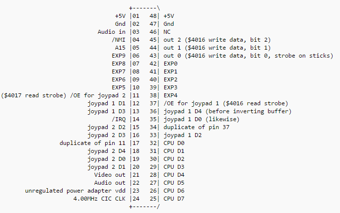
wiki.nesdev.com
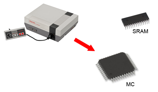
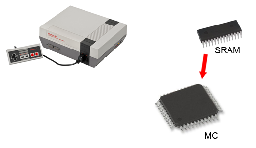
I use the combination of these to write to an external piece of SRAM shared with a microcontroller (MC). As the SRAM is written to by the NES; the MC grabs it and processes it. I have the NES writing a simple message protocol which can be one of two messages. The first is an “Echo” where the MC will write back (I.e. “echo”) a value to the NES, and the second is a “Tweet” where the MC will relay a tweet from the NES to a server over TCP/IP.
Here is the high level design:

NES writes a value to SRAM
NES signals the MC that it has updated SRAM
MC reads the value from SRAM

MC writes a value to SRAM (If warranted by the message)
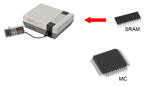
NES read the value from SRAM (If warranted by the message)
This blog is primarily going to cover how the NES interfaces with the external SRAM and the MC. Here are some other links which you might find helpful:
Go here for details on interfacing the MC with SRAM Go here for details on making a homebrew NES cartridge
NES to SRAM
The NES data bus is exposed in the expansion port through pins 25-32 which I simply wired to SRAM pins D0-D7. I wired the SRAM address lines A0-A15 straight to ground which effectively means the NES will always read and write to SRAM address $00. This is fine because after each byte is written the MC will grab it from the SRAM and vice versa. The SRAM is simply a temporary holding location for a single byte.
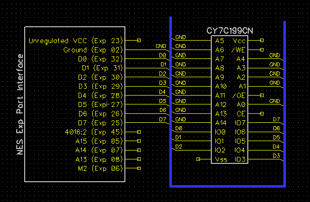
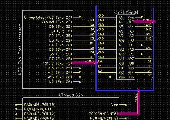
Next I needed to set the SRAM to read or write mode depending on whether the NES was going to read from it or write to it. SRAM has a write enable pin, if this pin is pulled low (grounded) the SRAM can be written to, otherwise it’s being read from. To toggle this I looked to pin 45 of the expansion port. The expansion port exposes 3 pins (43-45) which you can pull high or low through address $4016. Normally $4016 is used to access the joypad, but it has the advantage that the low three bits are also used to toggle these three pins. So I wired pin 45 to the write enable pin on SRAM. If I write $00 to $4016 that pulls the pin low, which sets SRAM to write mode; if I write $ff to $4016 it pulls the pin high which sets the SRAM to read mode. Additionally, I have also wired this to a pin on the MC. The MC queries this value to know if it needs to read a value the NES wrote or to write a new value for the NES to read. It’s worth mentioning that this does not interfere with the ability to read from the joypad. When $4016 is used to access the joypad you will not be doing SRAM reading or writing and vice versa.
Finally, I needed to enable the SRAM when the NES wants to interface with it. The SRAM can’t be enabled all of the time or it will interfere with the NES data bus and cause corrupted game data. SRAM has a chip enable pin which, when pulled low, will enable the SRAM. So I needed to wire up a signal to pull it low at the key moments the NES needs to read or write from it.
On a NES NROM cartridge board (Kung-Fu, Super Mario Bros, Baseball, etc.), addresses up to $4002 are for tile data, registers, etc.; while $8000 and above is used for code. $6000 is reserved for other purposes and maps to no where on these boards. This means I could leverage that address to trigger an SRAM enable anytime the NES wants to access it. Effectively this means a write to $6000 will enable the SRAM which in turn means it’s active on the NES data bus and, depending on read or write mode, it will read a value from the data bus or a write a value to the data bus.
How would $6000 work? The NES has 16 address pins (A0-A15), if they are all off (I.e. address $0000) they are all low which is 0000 0000 0000 0000; if they are all on (I.e. address $ffff) they are all high which is 1111 1111 1111 1111. As you can see, depending on the address the corresponding pins are high:
$4000 has A14 high (0100 0000 0000 0000)
$8000 has A15 high (1000 0000 0000 0000)
$6000 has A13 and A14 high (0110 0000 0000 0000)
So if A15 is low the NES is not accessing anything $8000 or above, which means it’s not accessing code. If A13 and A14 are high it’s not accessing anything below $6000 which means it’s not accessing tile data, registers, etc. As I mentioned before $6000 maps to nowhere on the NES cartridge so I can use that combination (A15 low, A13 and A14 high) to activate the SRAM.
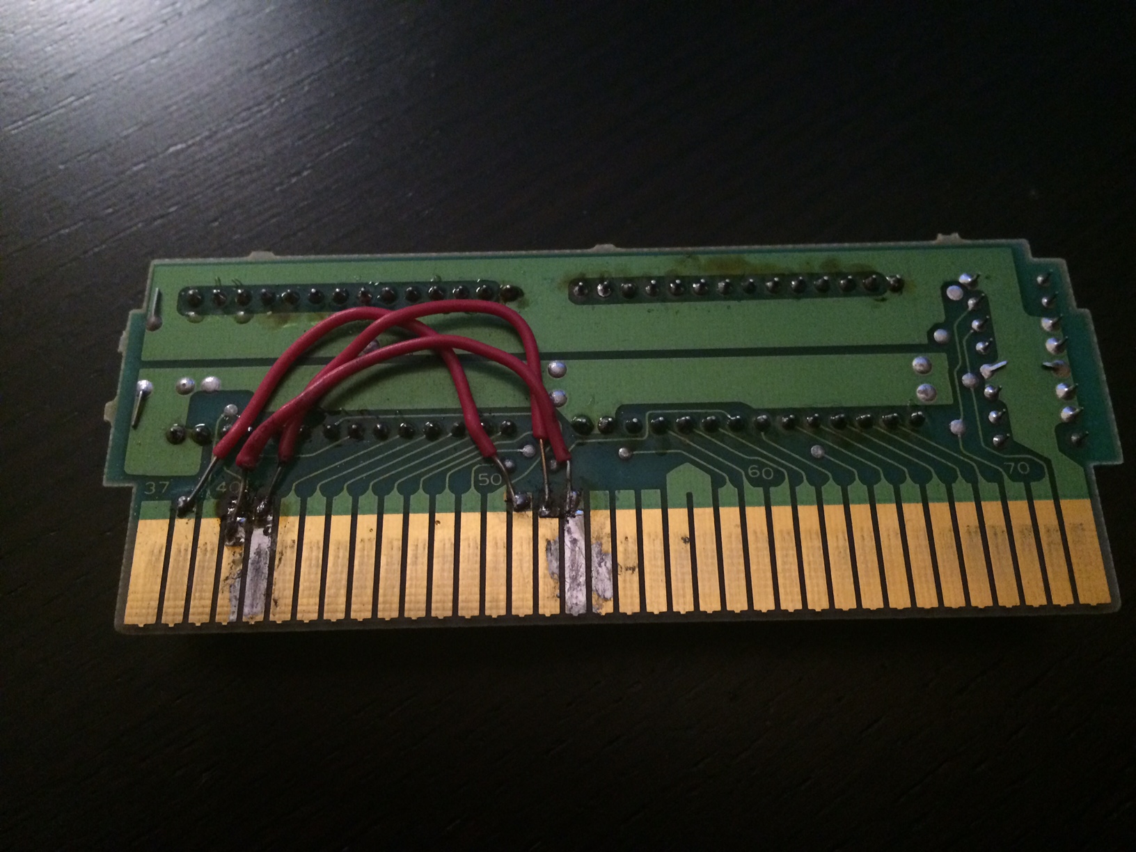
The expansion port already exposes A15 on expansion port pin 5, but I still needed to get A13 and A14. Fortunately the cartridge has unused pins 51 – 53 which pass through to expansion port pins 6 – 8. I had my dad come over and solder jumpers from cartridge pins 40, 41 (A13, A14) to cartridge pins 51, 52 thus passing those address lines through to expansion port pins 6 and 7. (My dad is a much better solderer than I am.)
One last item to note, the NES uses a modified 6502 chip. 6502 has alternating phases (called M2) which go high and low with each clock cycle. The data bus is only stable when M2 is high which means I need to make sure M2 is high when I enable the SRAM or it might read garbage values from the data bus. This means M2 must also be sent to the expansion port. M2 is exposed on cartridge pin 38, so my dad soldered cartridge pin 38 to cartridge pin 53 which passes through to expansion port pin 8.
Here is the final soldering job on the cartridge, thanks Dad!
Finally, I had everything I needed exposed on the expansion port. I ran those 3 address lines and the M2 line through an OR and NAND gate which resulted in a signal which goes low (to enable the SRAM) when A15 is low, A13 and A14 are high, and M2 is high. One final note on this, when the NES disables the SRAM the same line is used to trigger an interrupt on the MC so the MC knows the SRAM has an updated value from the NES.
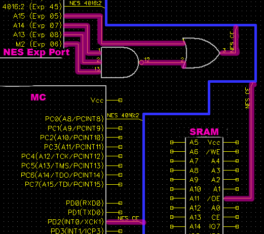
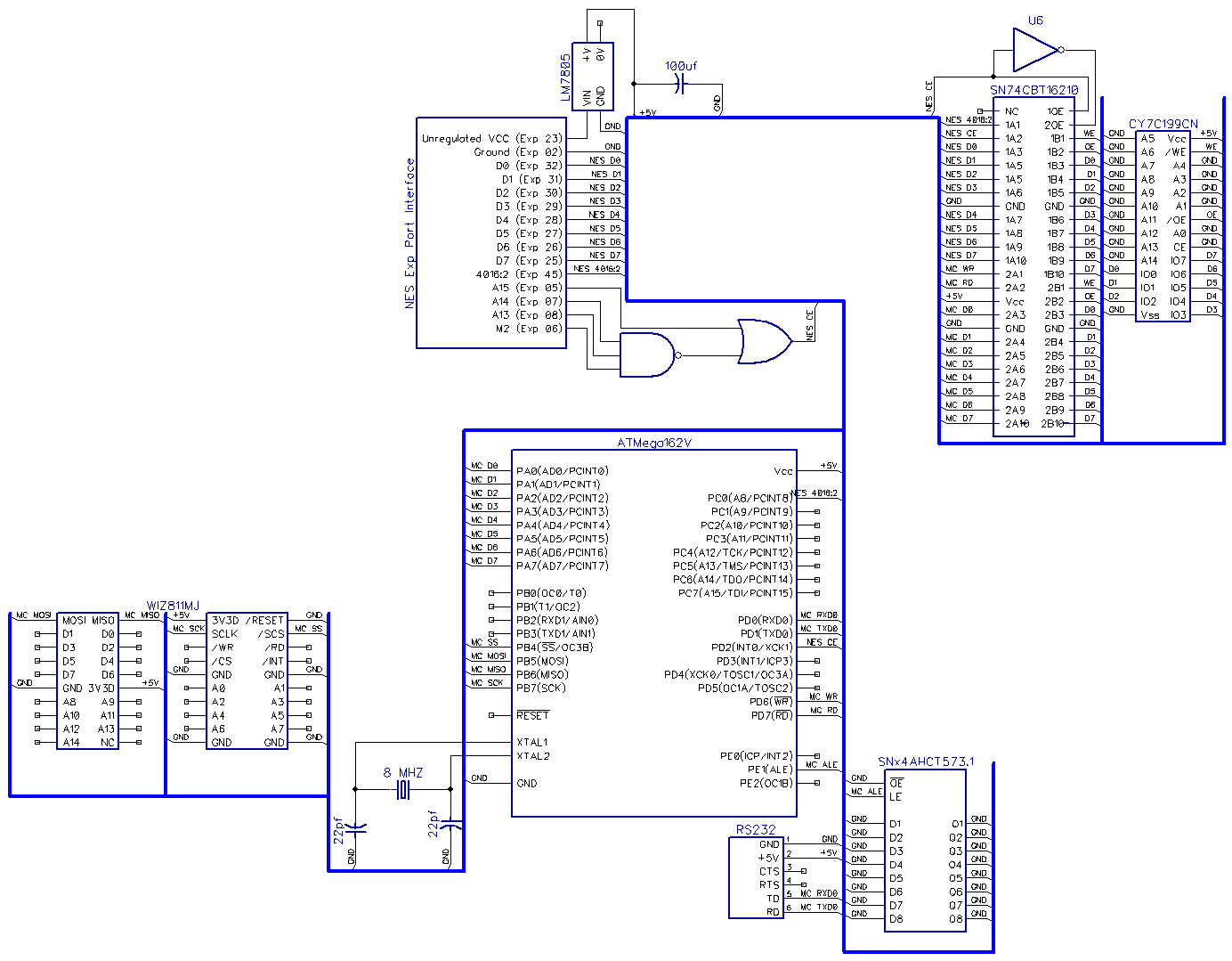
One flaw with my initial set up is that I needed to shut the NES lines off when the MC interfaced with the SRAM. To do this I routed the NES and MC lines through a BUS switch. When the NES enables the SRAM it also switches the BUS switch to its lines, at all other times the BUS switch is set to allow the MC lines to the SRAM. Here is the final schematic
NES Code
Communication Protocol
After each byte is written to SRAM by the NES, the bus is switched to the MC and the MC reads the byte in. The MC is expecting bytes to come in the format of Length|Command|Data, where Length is guaranteed to be 1 byte. This means the first byte the MC reads is the length (I.e. amount of bytes) the NES is planning to write, and then it continues reading until the length is fulfilled. Once the length is fulfilled it jumps to the second byte (I.e. the command) and dispatches the rest of the packet to the specified function (Tweet, Echo, etc.)
Sending the Tweet
When the the MC receives a Tweet command from the NES, it uses a TCP/IP chip to relay the Tweet to a custom server which uses the Twitter SDK to relay the Tweet to the world. Super special thanks to my brother Jered McFerron for writing the Twitter relay app on the server!
That’s It!
I hope this was interesting to at least 1 person out there. If you have any questions or insight please contact me!
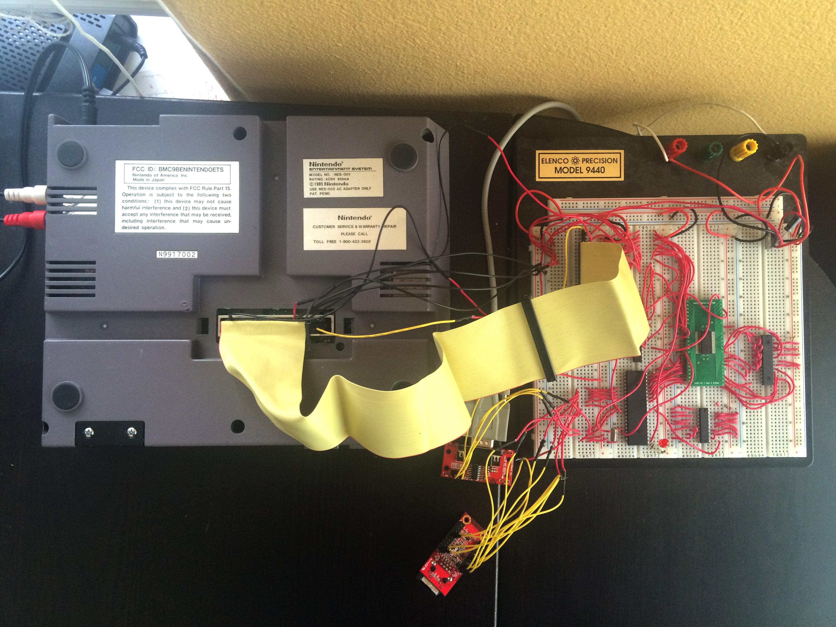
Here is the NES (upside down) with an IDE ribbon cable and a few extra wires coming from the Expansion Port to my breadboard:
The connector to the expansion port is an ISA connector cut down to 24 pins on each side and split in the middle to allow for a wider width.
Here is my custom NES cartridge
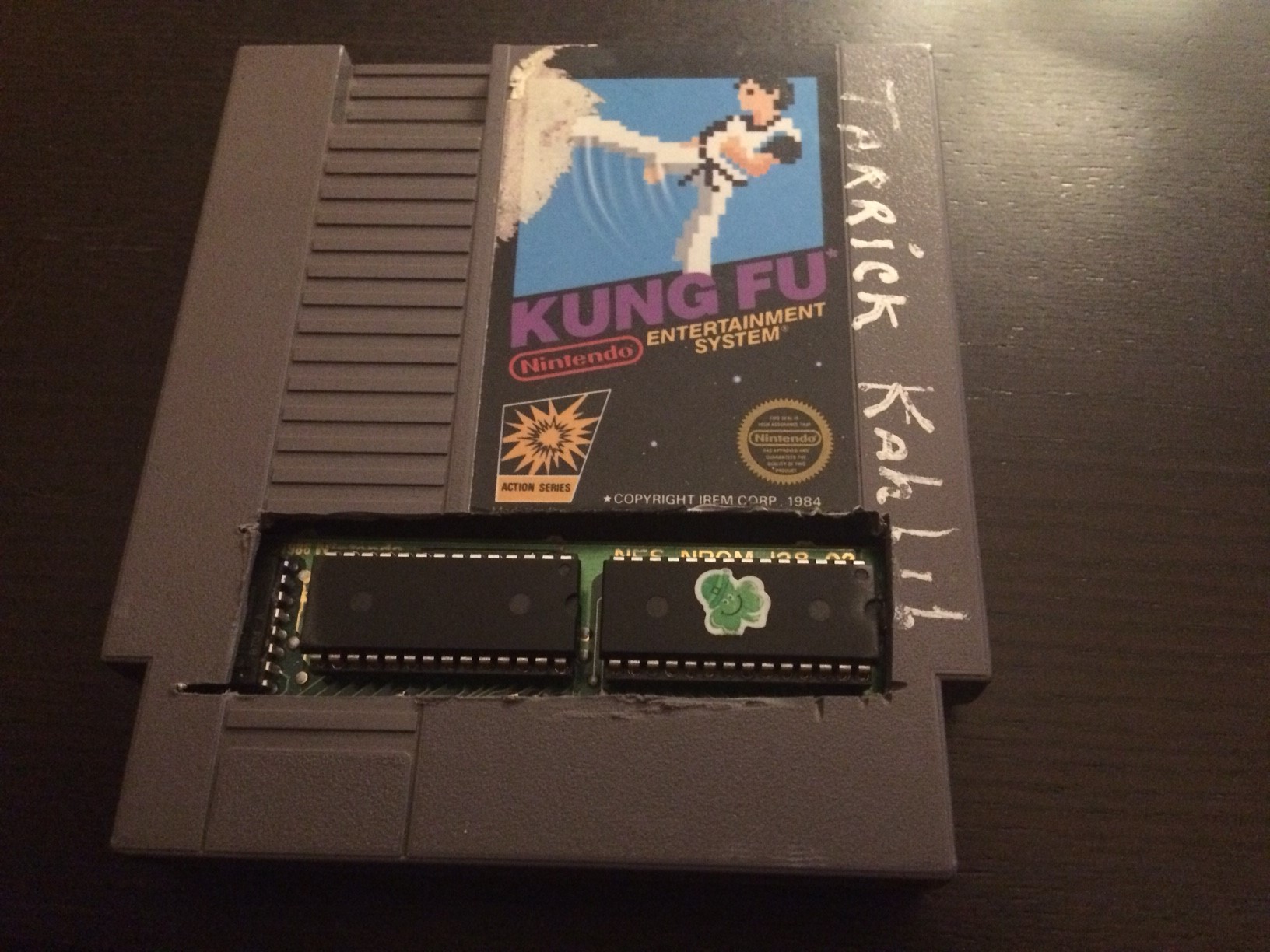
I have no idea who Tarrick is, but little did he know his game would be donated as a Twitter app 30 years later
Additional References:
http://wiki.nesdev.com
Expansion Port Pinout
Hardware:
ATMega 162V
Latch
BUS Switch
SRAM
OR Gate
NAND Gate
6502
TCP/IP